Schematic Capture And Pcb Layout Electronic Devices & Pcb De
Kicad pcb eda pcbnew routing Schematic capture define circuits connected process everything which The top schematic capture and pcb layout software for efficient designing
From the Capture schematic to the PCB layout - Page 3 of 7 - YouSpice
Electronic – resistors in paralel on pcb schematics – valuable tech notes What is schematic capture pcb layout? Download free kicad 7 schematic capture pcb layout
Schematic capture pcb layout
Kicad-6.0.5 : free download, borrow, and streaming : internet archiveSchematic capture diptrace pcb software layout schematics provides simulation Convert pcb layout to schematic in diptraceHow to turn a schematic into a pcb layout: pcb design for a custom.
Schematic capture and logical designFrom the capture schematic to the pcb layout Schematic capturePcb schematic demodulator.

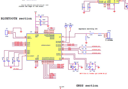
Pcb altium schematic schema outline control component creare databases efficiency improves convert components
Pcb layoutPcb entry pcd instructables eagle The top schematic capture and pcb layout software for efficient designingThe top schematic capture and pcb layout software for efficient designing.
Pcb wiring audio komatsuSchematic capture, pcb layout, pcba by hiberxen Download free kicad 7 schematic capture pcb layoutSchematic capture.

How to create a pcb layout from a pcb schematic in altium designer
Schematic capture and pcb layoutSchematic pcb layout inclinometer flexible turn custom into electrical articles circuit like schematics Pcb layout schematic mentor xpedition high expedition graphics routing speed placement designer environment addresses challenges important most dx updates screenSchematic capture services.
Schematic capture servicesElectronic devices & pcb development services — kickr design® Everything you need to know about free schematic capture and pcb layoutCreate pcb from schematic altium.

Free pcb schematic entry & layout software beat eagle for some features
From schematic capture to pcb layoutDesign circuits, schematic capture and pcb layout by muskyj Capture hytekHow to design a pcb layout.
Schematic captureKicad eda How to convert schematic diagram into pcb layout?Schematic capture software and pcb layout tools in altium designer| altium.

Schematic capture and pcb layout for manufacturing
Schematic capture eda pcb logical cadence circuit automation ema credit .
.


Schematic Capture Services

How to Turn a Schematic into a PCB Layout: PCB Design for a Custom

Download Free Kicad 7 Schematic Capture PCB Layout - Xtronic

Schematic Capture Pcb Layout
Services

The Top Schematic Capture and PCB Layout Software for Efficient Designing

Electronic Devices & PCB Development Services — Kickr Design®